TREND FOR
MINIATURIZATION
Techniques and practices used in compact camera design
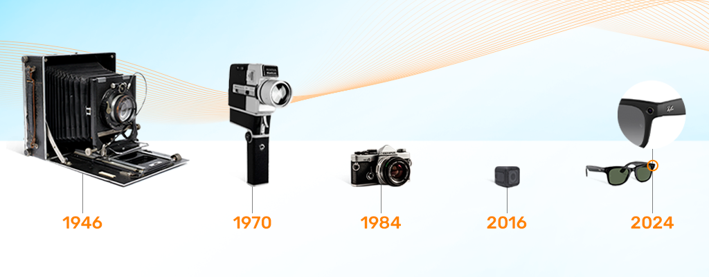
Historically, the technologies used in the design of consumer photo and video cameras were aimed at, among other things, reducing their dimensions. Today, this need is becoming even stronger, and in addition to the various requirements that customers have when discussing new projects with us, a major sticking point is the desire to make the final device small. This trend spans across different applications, from sports cameras or wearable gadgets to medical devices. The final products’ use cases are all different, but the goal remains consistent: to create a miniature turnkey camera, or a compact camera module that can be embedded into another device.
Requests for miniaturization make creating a consumer camera project quite challenging, as they require special attention to various domains. Let’s look at the key areas to consider when designing a compact camera system.
Streamlined system architecture and feature set
In every project, the customer first defines the concept of the product: problem, goal, constraints, environment, use cases, etc. Then, the concept is transformed into target device capabilities, such as video configuration, the ability to record and/or stream the content, operating time, and external interfaces. Based on these inputs, our Requirements Engineering (RE) and System Engineering (SE) teams clarify all key requirements and restrictions of the product, and create high-level system architecture, which focuses on an optimized set of software features, hardware components, and communication interfaces.
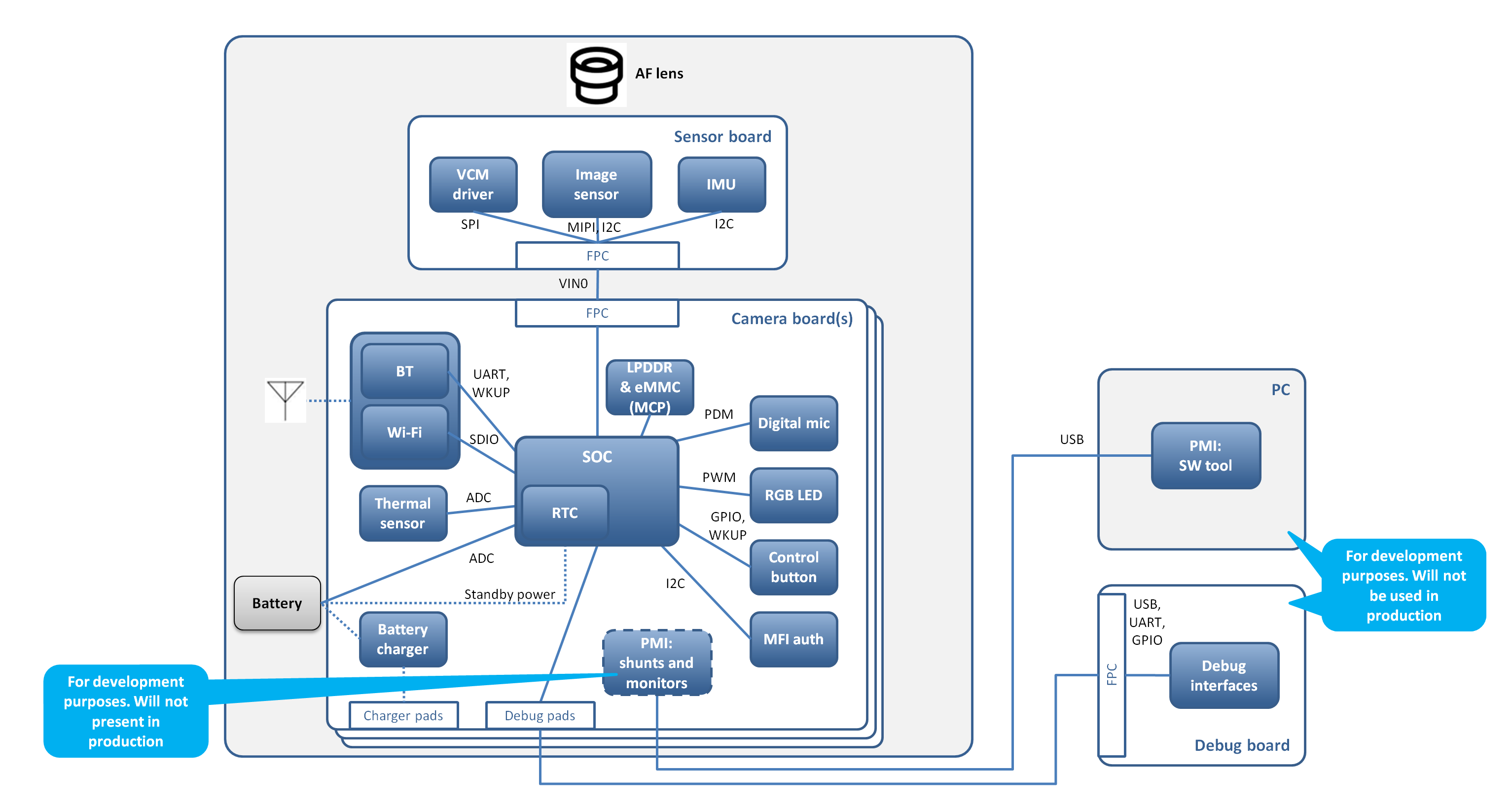
Pic.1: An example of wearable camera architecture
Proper components selection
It is worth mentioning that the selection of the right components plays quite an important role in the successful design of a compact camera. Having superior knowledge of the electronics parts available on the market, our Electrical Engineering (EE) and Peripherals teams propose a list of component candidates that are most suitable for the product, with the lowest possible form-factor and power consumption. Afterwards, our Procurement department works with multiple suppliers to obtain the suggested components at the lowest price and with the shortest possible lead time.
As a trusted Ambarella partner, Rhonda Software has access to their state-of-the-art Systems-on-Chips (SoCs), and also benefits from strong partnerships with leading image sensor and lens vendors. No matter what the camera is intended for, the Bill of Materials (BOM) will be filled with components that are optimal for the product, while taking into account the customer’s budget.
Complex-shape mechanical design and PCB composition of a compact system
The size and shape of a compact camera are primarily determined by how the camera will be mounted on or built into a particular “base” or “framework”. With deep understanding of this need, our Mechanical Engineering (ME) team creates a detailed drawing of the camera to best fit the constraints of the product’s industrial design. At this stage, the composition of the Printed Circuit Boards (PCBs) is determined, taking into account all mechanical limitations of the product. To make mass production of the final device more reliable and cost-effective, Design for Manufacturing (DFM) best practices are considered throughout the design process as well.
Take a look at the design example that represents a battery-powered consumer camera with full HD video recording, audio capture, Bluetooth connectivity, a gyro sensor, an LED, and a button for user interaction, all housed in a body measuring just 36x14x14mm.
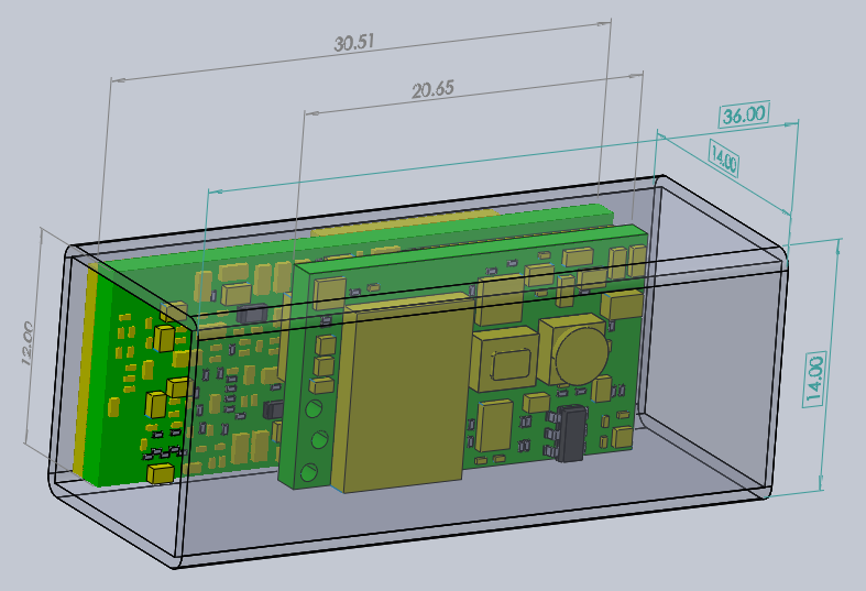
Pic.2: An example of a compact camera design
Dense PCB design
Next, our EE team uses all of their best knowledge to shrink each specific PCB to a size of tens of millimeters and match the target form factor, shape and thermal requirements. High Density Interconnects (HDI) design practices are widely applied to make each specific board in a camera truly compact. Dense component placement, large BGA and small-pitch component fan-out optimization, multilayer boards design, finer traces, and simulation of high-speed routing behavior are all well-known techniques that we employ in our camera projects. At the same time, the EE team ensures signal integrity and adherence to EMI/EMC measures, even in situations where general recommendations for high-speed routing cannot be met due to PCB space limitations.
For example, please look at our A12 System-on-Module (SOM) which represents a fully-functional camera design with integrated Wi-Fi, digital microphone, SD card slot, and multiple interfaces available via connectors on an 8-layer PCB as tiny as 44x31mm (which is almost half the size of a standard credit card).
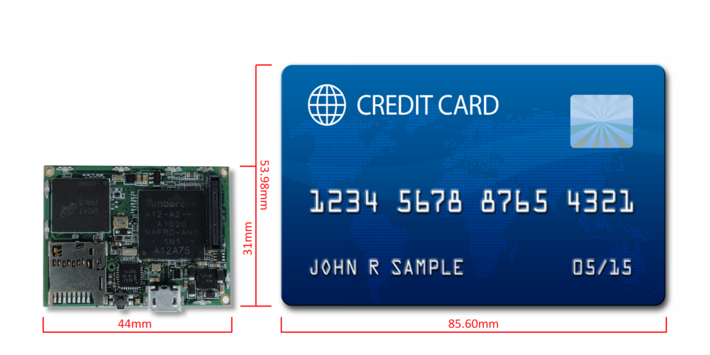
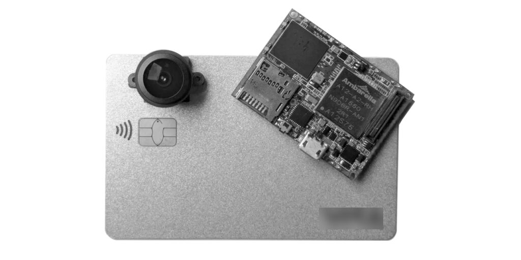
Pic.3: Size of A12 SOM compared to a credit card
Fine wiring
All PCBs and sub-modules are connected together, with special attention to the high-speed interfaces of the image sensor. Using a Flat Flexible Cable (FFC) or Flexible Printed Circuit (FPC) is the most adaptable approach, as their shape can account for the specific internal structure of the final device. Knowing the limitations of a specific product, we can design custom-shaped FPCs or rigid-flex PCBs to minimize the occupied space. When FPC cannot be used due to width constraints or one dimension’s flexibility, it can be replaced with micro-coaxial cables as an alternative option to keep data routes compact but reliable.
Slim optical sub-system
Getting a small yet top-grade optical module is another crucial step of miniature design. Without a doubt, using an off-the-shelf mobile sensor module is the most practical approach, but this only works if the module precisely meets the product requirements, planned production volumes are sufficiently high, and so on. Not every project can handle such constraints. As such, a good alternative is a custom-designed optical module, where the lens, image sensor, and other hardware components such as EEPROM, ALS, IMU, or a lens motor driver (if any) are packed in an even smaller space than the main PCB.
For some camera systems, just having the compact optical module is enough. This is especially true when considering the possibility of using SerDes technology to connect a module to a remote host. Here is an example of an optical module from our GMSL2 CAMERA EVK with the lens, image sensor, serializer, and automotive-grade FAKRA connector assembled in a 40x30x30mm case.
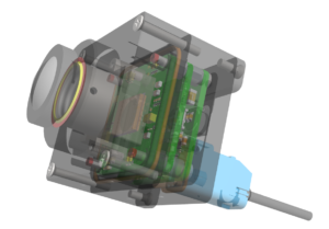
Pic.4: 3D model of the optical module from GMSL2 camera EVK
Custom lens for enhanced image quality
Size constraints make it difficult to achieve high-quality images, especially in low light conditions. As a result, in some camera design scenarios (particularly for ultra-compact or specialized smart vision devices) off-the-shelf lenses may not suffice. In these cases, we offer custom lens design services to create the smallest possible lens to suit the specific product’s needs. This custom approach is way more challenging, but the superior results are well worth it. Once samples are available, our Image Quality (IQ) experts rigorously validate them in our specialized IQ lab to ensure the lens meets all requirements for the camera project.
Thermal simulation challenges
With miniature design, it is challenging to apply standard heat dissipation approaches like heat sinks or intensive air flow. Using heat-conducting materials for camera housing typically helps solve the problem, but not in all cases. However, even a miniature design must remain compliant to temperature restrictions. Internal temperature should not exceed the operating ranges of hardware components, and the surface temperature should be acceptable from the standpoint of safety standards (i.e. IEC 62368-1). To meet these requirements, our ME team develops the thermal model of the device and performs the necessary thermal simulations.
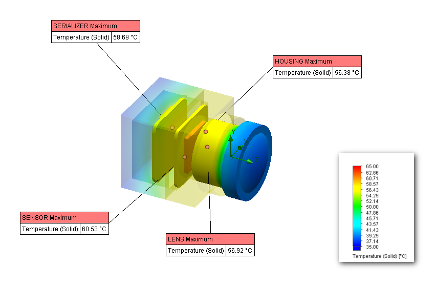
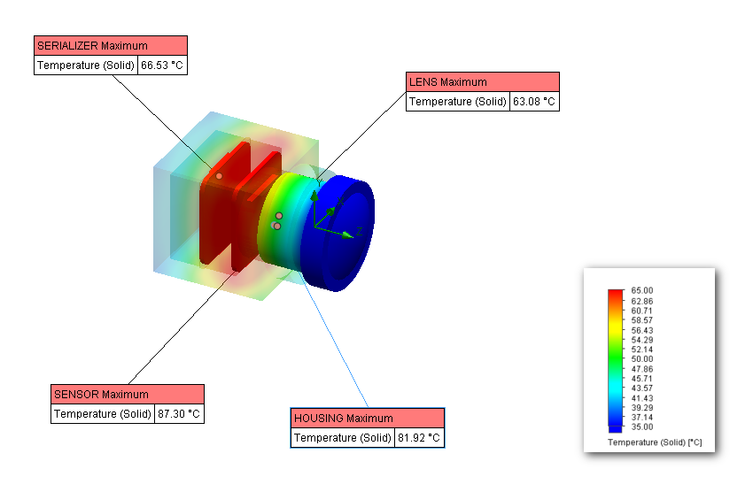
Pic.5: Thermal modeling for various camera design options
Achieving energy efficiency
Reducing power consumption remains the most effective option to avoid complex thermal and mechanical design. Selecting power-efficient components, properly designing power delivery circuits, and using optimal frequencies and configurations all contribute to reduced power consumption, which is especially critical for compact devices.
In addition, Rhonda Software has designed an in-house technique to validate and optimize system power consumption – the Power Measurement Instrumentation (PMI) tool. Using this tool, we can examine any of the device’s power rails in both highly-loaded and sleep use cases, enabling highly accurate analysis of power consumption in various camera system configurations.
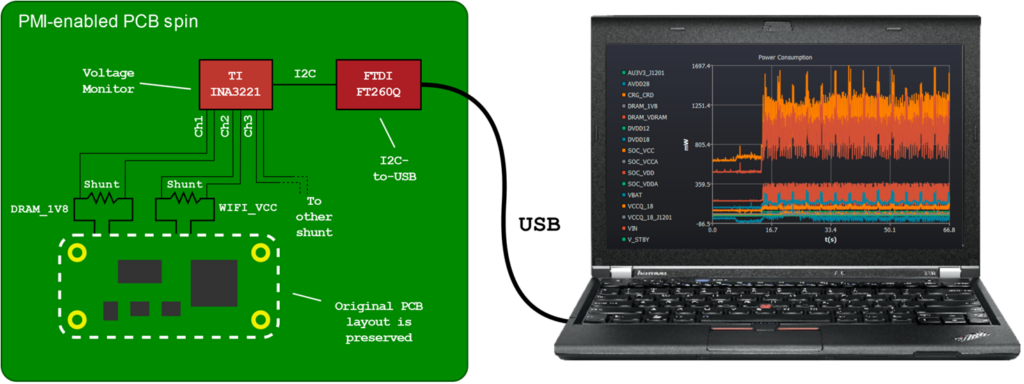
Pic.6: The structure of the PMI tool
Creating Innovative Camera Designs with Rhonda Software
We have mentioned our most-typical practices, but that’s not all. Every project brings unique challenges, and encourages us to seek uncommon trade-offs between constraints imposed by the end product's purpose and the customer’s desired features.
With all that said, Rhonda Software approaches product design by meeting the most demanding requirements for size, performance, and functionality in various camera system applications. Our expertise in custom camera development, combined with our readily available PCB designs, strong supplier relationships, and experienced team, allows us to confidently tackle the most challenging aspects of your compact camera project.
We would be happy to help you with your next camera innovation. Contact us to explore how our expertise can turn your miniature device concept into reality!